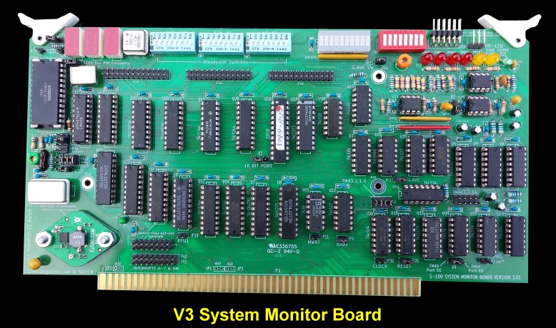
As always, first examine the bare board carefully for scratches or damaged traces, use a magnifying glass if need be. The quality of the boards we get is excellent. I must have done
50 by now, never had a problem, but there is always a first time. A broken trace is almost impossible to detect by eye on a completed board.
I find it useful to carefully slide a file at 45 degrees along the edges (front
& back) of the S100 connectors for easier insertion into the bus. Carefully, just
one or two strokes.
Next solder in all the required IC sockets, resistors, resistor arrays, capacitors, jumpers,
switches and the 5V voltage regulator. Because this board utilizes a
fair amount of power to drive the Hex displays so I prefer to use a 78H05
regulator. Be sure you put the two resistor arrays are in with the correct orientation of pin 1. Check their values before
soldering (they are difficult to remove).
For prototype boards I generally use "double swipe" IC sockets. For a critical board like this I prefer to use "Machine Tooled" IC sockets. However they are more expensive and you have to be particularly careful not to bend the IC pins.
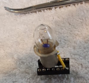
Next insert all 7 LED's. Before soldering them in place ground the appropriate pin on the U33,
U3, U29 and U26 sockets to make sure it lights up. I use blue for
System tick,, yellow for Reset and Slave Clear and red for the 4 TMA
lines.
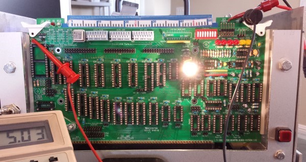
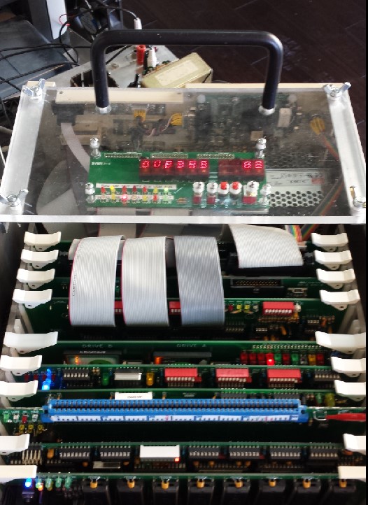
Check the voltage to sockets on the board is above 5V by placing the board
in your S-100 system using an extender board. With no load you will
typically get 5.00V (+/- 0.25V). BTW, your system should boot and run
correctly with its Z80 master CPU board. If not, you have a serious solder
bridge somewhere on the board. Before you do anything else with a
magnifying glass go over every socket on the board and examine for a proper
solder joint. I like to "reheat" each joint just to be on the safe side. The
silk screen/varnish on these boards us quite thick. It's easy not to have a
good solder joint for the ground pins. Double check. Extra time here will
save you hours later, (been there done that! ).
We will now build the board up in functional steps.
Avoid the temptation of adding everything at once and popping it into
your S-100 box. Step by step is faster in the end -- trust me.
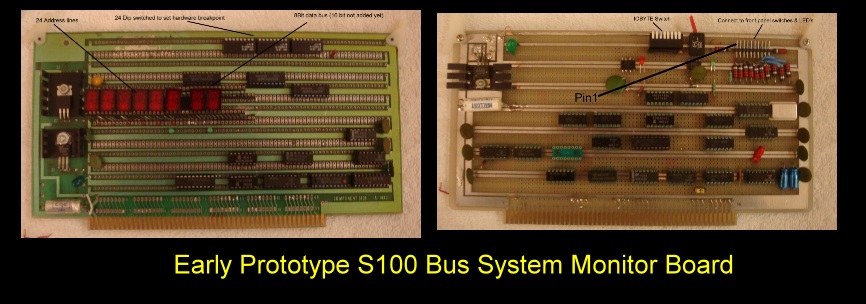
This assembly instruction assumes you have the earlier (V1) board and
will be using one of the mezzanine boards that came with it. If
not build one of those boards first.
Install the 2MHz Oscillator. You can solder this one in it will never
need to be changed.
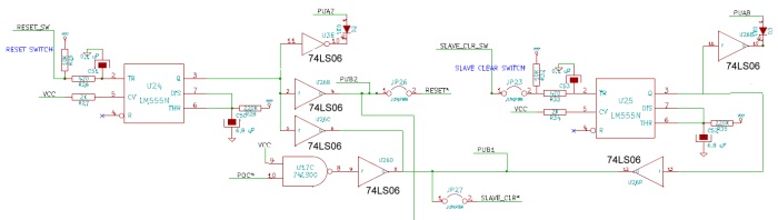
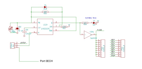
First we will install the reset, slave clear and system tick
circuits.
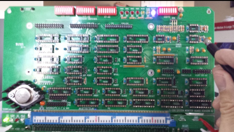
Install the three 555's , U24, U25 & U29.Add U17, U26, U36 & U3. Insert JP23, JP26 & JP27.
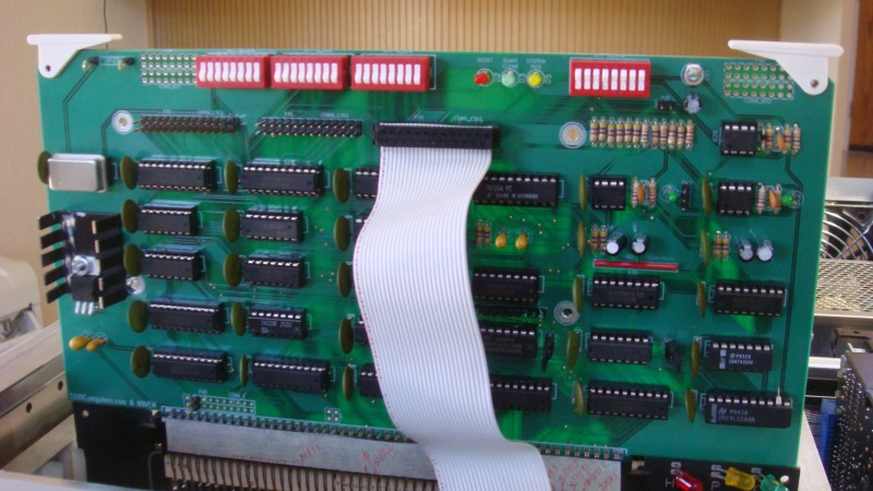
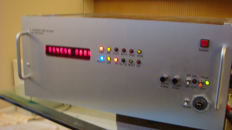
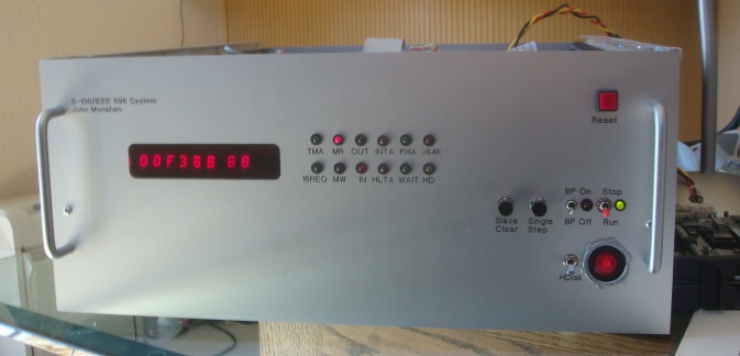
Insert the board into your system and power up. The System tick LED D5 should be
flickering. Grounding pin 12 of P39 should light up the reset LED
(D2). Grounding pin 18 of P39 should light up the Slave LED (D3). Here
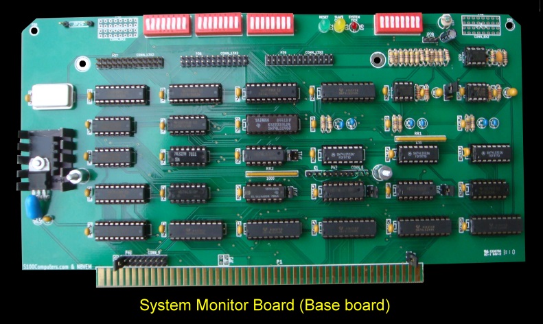
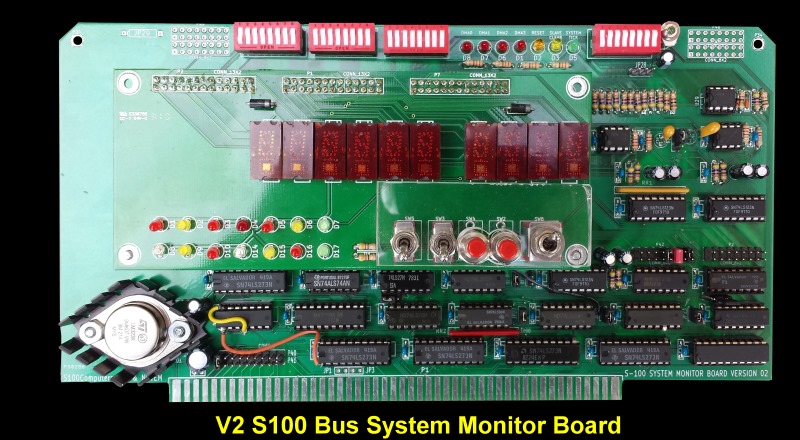
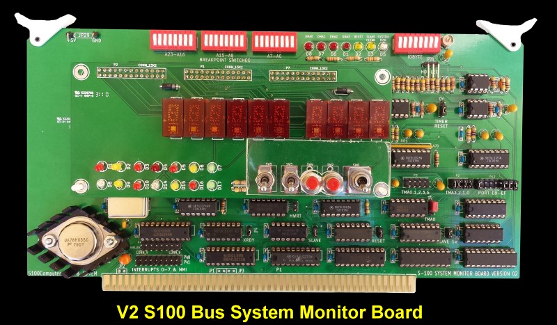
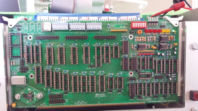
is a picture of the board at this stage:-
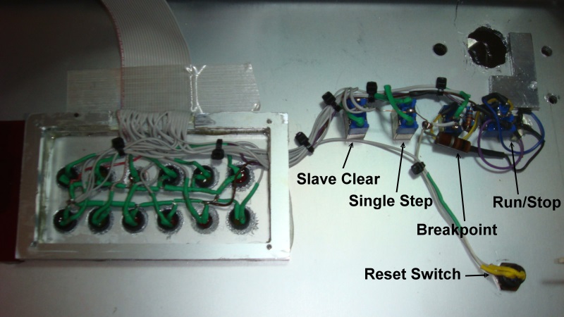
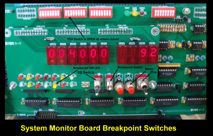
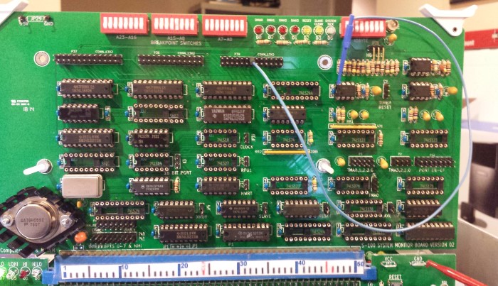
Next we will add the breakpoint, stop and single step circuit.
Add U22, U18, U16, U15, U14, U8, U9, U11, U19, U20, U21, U7 & U10.
Insert jumper JP4.
Insert the board into your system and power up.
Then carefully ground pin 14 of P39.
We will set a breakpoint in RAM at 800H. So set all the breakpoint switches
to closed except switch 5 of SW4.
In your monitor display RAM 0 to FFFFH. The CPU should stop just
before 800H is displayed. Later you can single step from this point
onwards.
Note the ground connection on pin 14 should be made after the Z80 monitor
signs on. This is because our
Z80 CPU board on power
on, scans the address lines from 0 up, to find the monitor ROM at
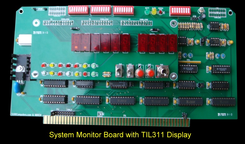
F000H. It would pass through 800H and lock up. Here is a picture of
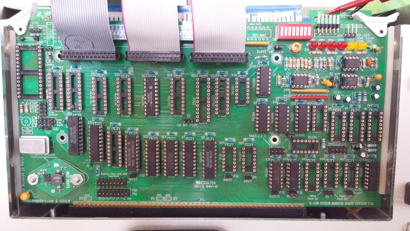
the board at this stage:-
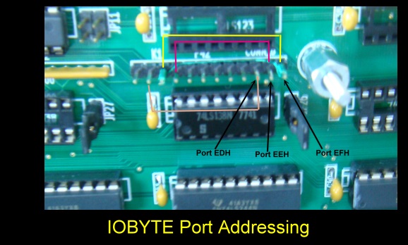
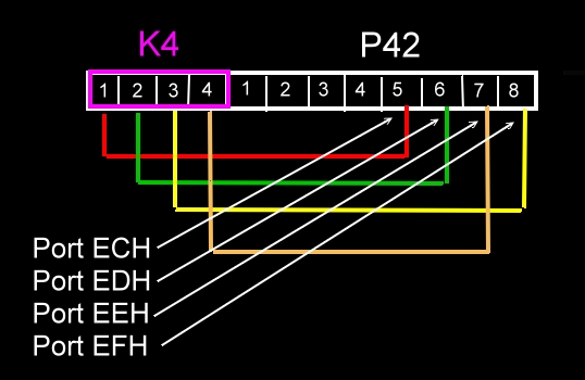
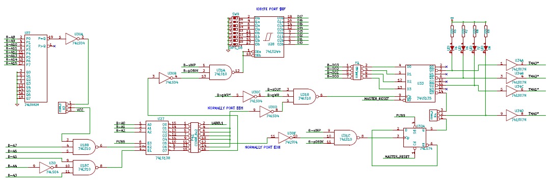
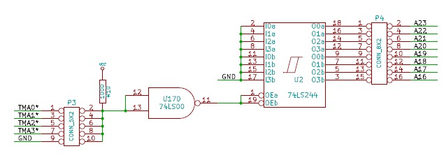
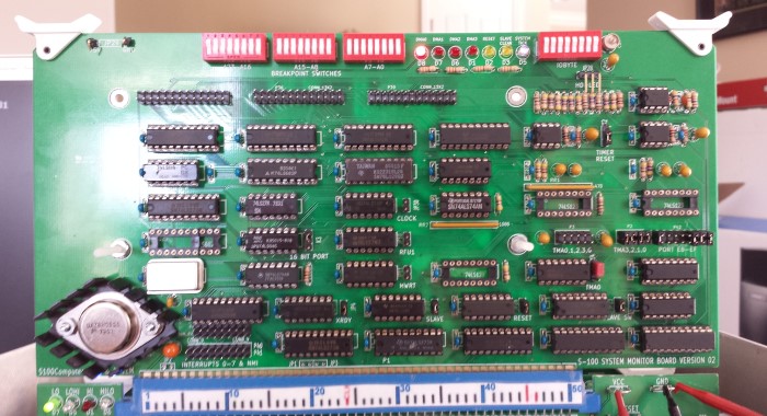
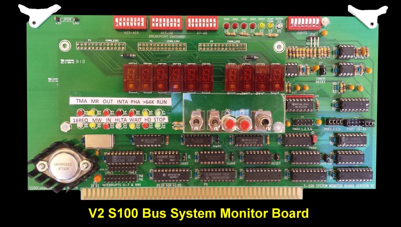
Next we will add the IOBYTE port and TMA selection circuit.
Add U37, U18, U27, U31, U28, U32, U33, U34, U27, U12, & U13.
Jumper K3, 1-2. Jumper K2 2-3. For P2 connect 1-2, 3-4, 5-6 & 7-8

.jpg)
.jpg)